
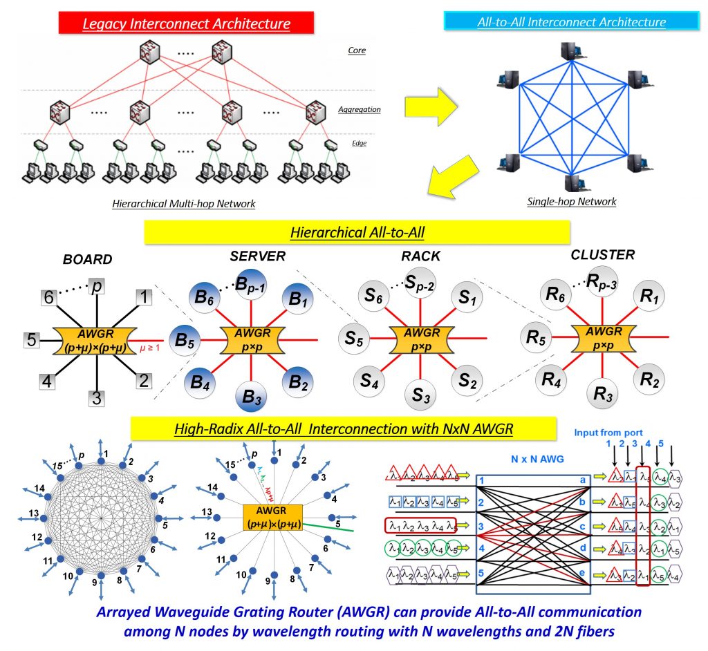
Project Overview
Data centers and High-Performance Computing (HPC) systems are an essential part of our cyberinfrastructure. While the energy consumption of data centers worldwide is currently estimated at 26 GW, the amount of data we process is growing at ~2 dB per year. Unless we drastically improve the energy efficiency, the energy consumption in data centers worldwide will increase to ~2600 GW in the next decade. Unfortunately, traditional electronic data center designs today remain inefficient in energy utilization due to poor efficiency in electronics and poor communication architectures. Due to limitations in port-count and bandwidth of the electronic switches, the inefficiency of the cascaded switch stages compounds, especially in terms of latency, throughput, scalability, and power consumptions. Utilizing the classical electronic infrastructure current and future data centers are not going to achieve the 20-30MW expected results in terms of energy in 2020 [1, 2]. Current HPC Data Centers use a single architecture (e.g. 3D Torus [3], HyperX [4], and Fat-Tree [5, 6]) to serve various applications. To improve the performance and efficiency of these systems, it is important to observe that multiple heterogeneous applications running inside HPC Data Centers present different communication patterns among the computing nodes. To optimize each application performance, it would be desirable to match the inter-node communication network to the specific application [7]. Hence, the best design should be capable of reconfiguring the network based on various communication patterns of heterogeneous applications. Such reconfiguration is difficult in electrically interconnected systems with fixed cabling but it can be possible when using integrated optical switching technologies as passive and active wavelength-routing in Arrayed Waveguide Grating Routers (AWGRs) [8, 9].
The energy cost of moving data, particularly for long distances and high data-rates, is becoming one of the dominant factor for the energy consumption, greater than the computational energy cost. Furthermore, a significant part of power inefficiency in communication comes from poorly adapting to the communication and traffic patterns. Hence, most of the time, current communication systems are consuming energy even when no meaningful bits need to be transported. This means that most of the energy consumption in current data center architectures, is quite independent of the load, and thus load balancing/scheduling techniques cannot guarantee significant energy savings. Finally, close integration of photonics with electronic ICs, or ‘embedded silicon photonics’ is viewed as a transformational technology which enables energy-efficient, high throughput, and cost-effective data communications. By introducing embedded photonics it is possible to intimately integrate photonics and electronics via optical interposers and silicon photonics with 2.5D and 3D integration. Embedded photonics will significantly impact the energy efficiency and the cost of chip-to-chip, board-to-board, and rack-to-rack data communications.
Current Research Activities
This project pursues scalable, high-throughput and energy-efficient computing systems realized by incorporating high-radix silicon photonic switches, multi-socket blade integration, application-aware reconfigurability of interconnection topology and resource management. In particular, UC Davis research team has been pursuing the following research efforts:
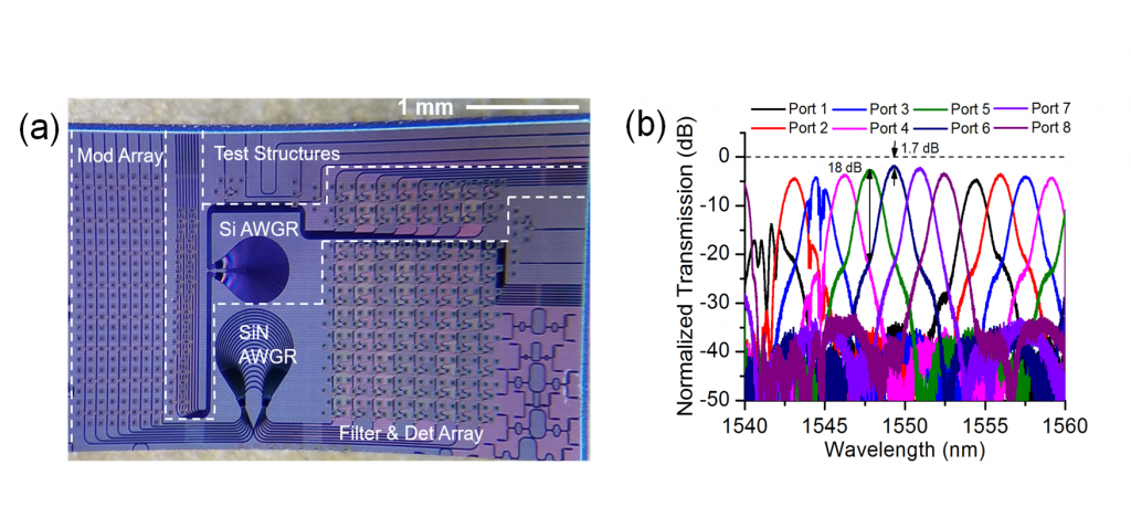
1. Design, fabrication and testing of high-radix silicon photonic switches exploiting contentionless wavelength routing in arrayed waveguide grating routers (AWGRs) as a building block for all-to-all interconnection inside a multi-socket blade (MSB). Through the reconfigurability of the AWGR switch we will achieve reconfigurable optical interconnection between the MSBs depending on the application needs.
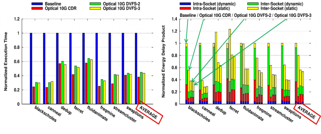
2. Development of a scalable system-wide benchmarking simulator for optimizing (and reconfiguring) the interconnection topology and resource allocations for given (dynamically changing) applications, including energy-efficient communication by making use of dynamic frequency and voltage scaling (DVFS).
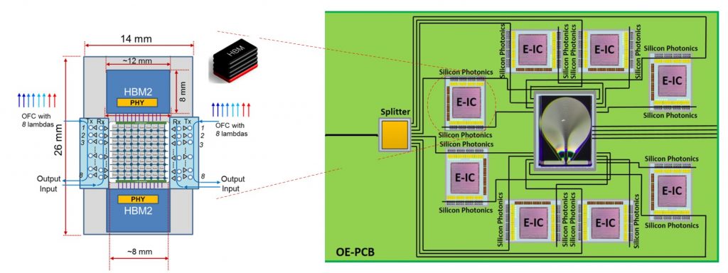
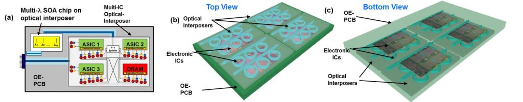
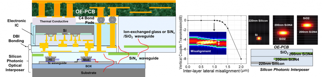
3. Optical-electrical printed circuit board (OE-PCBs) and interposers that exploit 3D photonics coupled to silicon photonic switches and transceivers, thus achieving photonic and electronic interconnects between electronic ICs and silicon photonics.
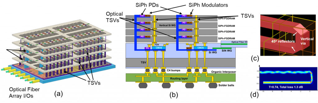
4. Design, simulate, and develop DRAM with embedded 3D electronic-photonic-integrated-circuits (3D EPICs) for 4x reduced latency and 4x reduced power consumption in processor-memory average access time (AMAT) interconnected by AWGRs. Figure 12 shows details of the configurations of SiPh-FGDRAMs. The Optical TSV is based on the 3D silicon photonics recently experimentally demonstrated the PI’s group [28]. As Figure 12 (c) illustrates, the Optical TSV consists of 90 degree vertical couplers and vertical U-turn silicon photonic devices which consist of a silicon photonic vertical via and a 45o reflector attached to a waveguide end. This vertical coupler can also be used for interlayer coupling in a multi-layer silicon photonic 3D integrated circuit by placing a matching vertical coupler face-to-face.
References
1. McMorrow, D. and M. Corporation, Technical Challenges of Exascale Computing. 2013: MITRE Corporation.
2. Kogge, P.M. and T.J. Dysart, Using the TOP500 to trace and project technology and architecture trends, in Proceedings of 2011 International Conference for High Performance Computing, Networking, Storage and Analysis. 2011, ACM: Seattle, Washington. p. 1-11.
3. Horiguchi, S. and T. Ooki. Hierarchical 3D-torus interconnection network. in Parallel Architectures, Algorithms and Networks, 2000. I-SPAN 2000. Proceedings. International Symposium on. 2000. IEEE.
4. Kim, J., et al. Technology-driven, highly-scalable dragonfly topology. in ACM SIGARCH Computer Architecture News. 2008. IEEE Computer Society.
5. Chia, M.C., et al., Packet Loss and Delay Performance of Feedback and Feed-Forward Arrayed-Waveguide Gratings-Based Optical Packet Switches With WDM Inputs-Outputs. Journal of Lightwave Technology, 2001. 19(9): p. 1241 – 1254.
6. Al-Fares, M., A. Loukissas, and A. Vahdat, A scalable, commodity data center network architecture. SIGCOMM Comput. Commun. Rev., 2008. 38(4): p. 63-74.
7. Bienia, C., S. Kumar, and K. Li. PARSEC vs. SPLASH-2: A quantitative comparison of two multithreaded benchmark suites on Chip-Multiprocessors. in Workload Characterization, 2008. IISWC 2008. IEEE International Symposium on. 2008.
8. Kamei, S., et al., 64 x 64-channel uniform-loss and cyclic-frequency arrayed-waveguide grating router module. Electronics Letters, 2003. 39(1): p. 83-84.
9. Glance, B., I.P. Kaminow, and R.W. Wilson, Applications of the integrated waveguide grating router. Lightwave Technology, Journal of, 1994. 12(6): p. 957-962.