
Project Overview (Check the SpiderZoom video from Lockheed Martin)
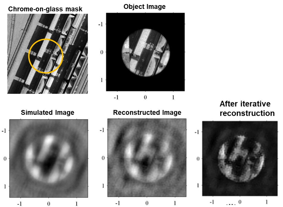
The interferometry techniques use superimposed electromagnetic waves to extract information of the wave source[1, 2]. In astronomy, an interferometer uses far-field spatial coherence measurements to extract intensity information from a source to form an image. Examples include the Very Large Telescope Interferometer, the Navy Precision Optical Interferometer, and the Very Long Baseline Interferometer. These systems use meter-class telescopes to collect light and have interferometer baselines on the order of 10 m ~100 m. Often, measurements are made only using a few telescopes at a time over long imaging campaigns. Complex beam combination systems with long adjustable delay lines are needed for optical path length matching when viewing objects in different parts of the sky. Recently, we proposed the concept of a Segmented Planar Imaging Detector for Electro-optical Reconnaissance (SPIDER)[3-6]. SPIDER is a small-scale interferometric imager that uses a lenslet array to simultaneously form many interferometer baselines and photonic integrated circuits (PICs) to miniaturize the beam combination hardware. Simultaneous measurements on several baselines in two dimensions will eventually enable snapshot imaging. By designing SPIDER as a common mount system, with a fixed boresight for each lenslet, the beam combination hardware can be greatly simplified by eliminating the need for long adjustable delay lines. The whole system can be rigidly pointed to look in different directions. Our long-term goal is to develop SPIDER as an alternative to conventional optical telescopes. Consisting of large optics, supporting structures, and precise thermal controls, conventional optical telescopes can be bulky, heavy, and power consuming. For instance, the Hubble telescope has a total mass of 27,000 pounds, its primary mirror is 2.4 m across, and the telescope is 13.3 m long. The interferometric imaging telescope of the same diameter (baseline) can achieve the same resolution but avoids the need for large lenses or reflectors contained in a large tube structure that must maintain a rigid structure across the ambient temperature range. The interferometric imaging telescopes based on PICs have the potential to reduce the size, weight and power (SWaP) compared to a conventional telescope with similar effective aperture and spatial resolution. The SPIDER concept, illustrated in Figure 1 describes a Fourier-domain interferometric imaging telescope that utilizes photonic integrated circuits (PICs) to directly detect white-light interference patterns. Light from a scene is coupled through multiple pairs of separated lenslets into waveguides on a PIC chip and combined to form the interference pattern. By measuring the interference pattern from these baselines, the intensity distribution of the scene can be reconstructed.
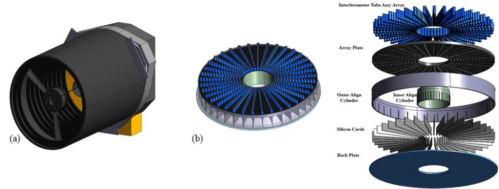
Figure 1. (a) Traditional telescope based on bulky optics (b) Proposed photonic integrated circuits imager system based on SPIDER concept. (c) Photonic Integrated Circuits imager system based on SPIDER concept design (exploded view): Assembly Arrays, Array Plate, Aligning Cylinder, PICs and Back Plate from top to bottom [4].
This project pursues design, fabrication, and demonstration of a photonic integrated circuit (PIC) capable of conducting interferometric imaging with multiple baselines around λ = 1550 nm. In particular, UC Davis research team has been pursuing the following research efforts:
1. Design, fabricate, and characterize a silicon nitride (Si3N4) multilayer platform optimized for low-loss and compact multilayer photonic integrated circuits[7].
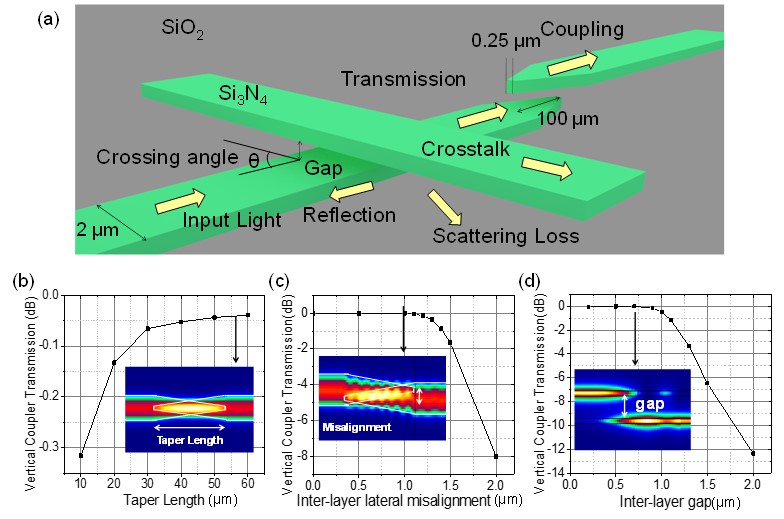
Figure 2. (a) Schematic of multilayer platform including tapered vertical coupler and waveguides crossing; (b-d)vertical coupling simulation of devices with varying (b) taper length,(c) lateral misalignment, and (d) inter-layer gap.
2. Design, fabricate and characterize of PIC components for interferometric imaging, such as low loss waveguide, MMI, thermal-optics phase tuner, and arrayed waveguide grating (AWG).
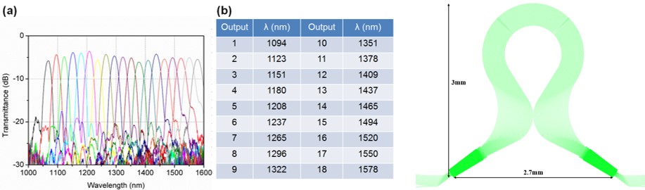
Figure 2. (a) Measured 18 channel 3.3THz channel spacing Si3N4 AWG spectrum. (b) Center wavelength of all 18 output channels. (c) The AWG layout on a 150nm Si3N4 waveguide platform.
3. Construct an optical testbed to generate an extended scene and illuminate the PIC, then test the PIC’s image-forming capabilities.
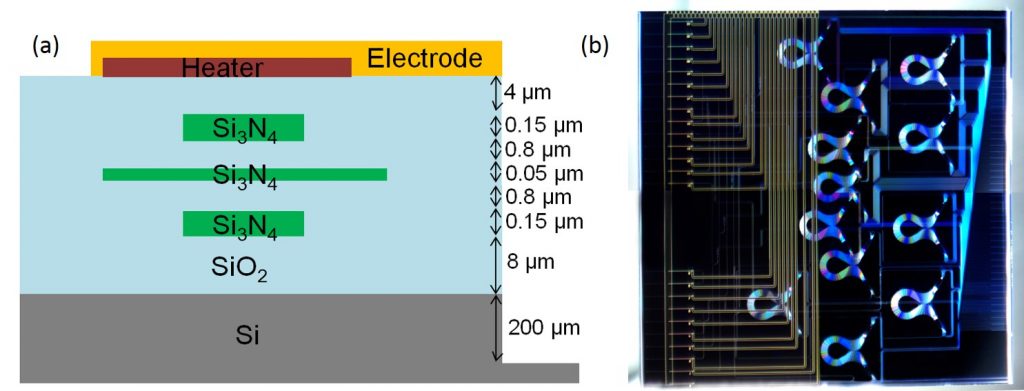
Figure 4 (a) Cross-section view of fabricated multilayer Si3N4 PIC. (b) Multilayer Si3N4 PIC containing functional devices such as AWGs, MMIs and thermal-optics phase tuners.
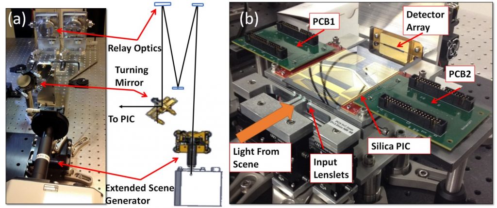
Figure 5 (a) Photo of the extended scene generator and its schematic diagram showing the optical beam path. (b) Photo of the packaged PIC on its holding. The PIC is shown in the center with the lenslets at the front, the detector array at the back and the two PCBs on the side.
References
1. Goodman, J.W., Statistical optics. 2015: John Wiley & Sons.
2. Hariharan, P., Optical interferometry. 2003: Academic
3. Su, T., et al., Experimental demonstration of interferometric imaging using photonic integrated circuits. Optics Express, 2017. 25(11): p. 12653-12665.
4. Thurman, S.T., et al. System Design for a SPIDER Imager. in Frontiers in Optics 2015. 2015. San Jose, California: Optical Society of America.
5. Scott, R.P., et al. Demonstration of a photonic integrated circuit for multi-baseline interferometric imaging. in Photonics Conference (IPC), 2014 IEEE. 2014. IEEE.
6. Kendrick, R.L., et al. Flat panel space based space surveillance sensor. in Advanced Maui Optical and Space Surveillance Technologies (AMOS) Conference. 2013. Maui, Hawaii.
7. Shang, K., et al., Low-loss compact multilayer silicon nitride platform for 3D photonic integrated circuits. Optics Express, 2015. 23(16): p. 21334-21342.8. Su, T., et al., Interferometric imaging using Si3N4 photonic integrated circuits for a SPIDER imager. Optics Express, 2018. 26(10): p. 12801-12812.
8. Su, T., et al., Interferometric imaging using Si3N4 photonic integrated circuits for a SPIDER imager. Optics Express, 2018. 26(10): p. 12801-12812.