INTRODUCTION
Large-scale computing platforms, also called warehouse-scale computing, have significantly transformed our lives over the past decades. Emerging applications are even more data intensive. However, scaling to an exascale system for both floating-point (e.g. for climate modeling) and fixed-point (e.g. deep neural network for pattern recognition) are facing severe challenges since the Dennard’s power-scaling law failed to keep up with the Moore’s law in 2006.
NEUROMORPHIC COMPUTING WITH NANOPHOTONICS
Recently, bio-inspired neuromorphic hardware systems such as IBM’s TrueNorth based on low-leakage 28 nm CMOS technology achieved 176,000 times higher energy efficiency than a state-of-the-art computing system based on a von-Neumann architecture . However, this and most of the other approaches accompanied the following shortcomings:
- The hardwares could only do what it was trained to do, and the training processes were time/energy consuming.
- Electronic solutions include long electrical wires with large capacitance and high interconnect energy consumption; the TrueNorth chip running at slow speeds consumed 2.3 pJ/bit with an additional 3 pJ/bit for every cm transmission.
- Electronic interconnect topologies are typically in four directions and required a number of repeaters.
- Limited scalability owing to the 2D interconnection topology with a single hierarchy.
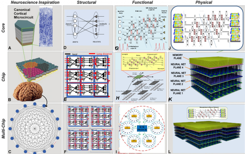
In a recent article , D.A.B. Miller reviews attojoule photonics and practical ~ 10 fJ/b interconnect solutions exploiting quantum impedance conversion where signal transmission need not be subject to charging of capacitance but rather exploit close integration with electronics with ~1 fF capacitance. This 10 fJ/b energy efficiency assumes ~19 dB (80x) link loss budget and ~30% wall plug efficiency of the light source. Hence, if such a nanophotonic repeater is integrated with electronics to form a neuron with a fanout of 10-100 on low-loss waveguides, it is conceivable to realize a nanophotonic neuron capable of communicating with other neurons at ~10 fJ/b nearly independent of the communication distance. Further, through 2D and 3D photonic integrated circuits with reconfigurable nanoMEMS (NEMS) photonic interconnection fabric, we can form hierarchical synaptic interconnection with changing weight values remembered by latching NEMS component while consuming little static energy. A combination of nanophotonic-nanoelectronic-NEMS technologies can possibly lead to a bio-inspired neuromorphic computing system as illustrated in Figure 2.
A. Nanophotonic Neurons
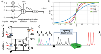
As illustrated in Figure 3, a nanophotonic neuron including the spiking nanoelectronic circuit can acquire the necessary functionality (spiking, integration, thresholding, reset) when synaptic connections are made with other neurons. A nanophotonic light source (e.g. a nanolaser or a nano-LED) and nanophotonic detectors will be integrated very closely with nano-transistors to achieve quantum impedance conversion. We expect ~ 10 fJ/b operation with ~80× fanout.
B. Nanophotonic-NEMS Synaptic Neural Networks
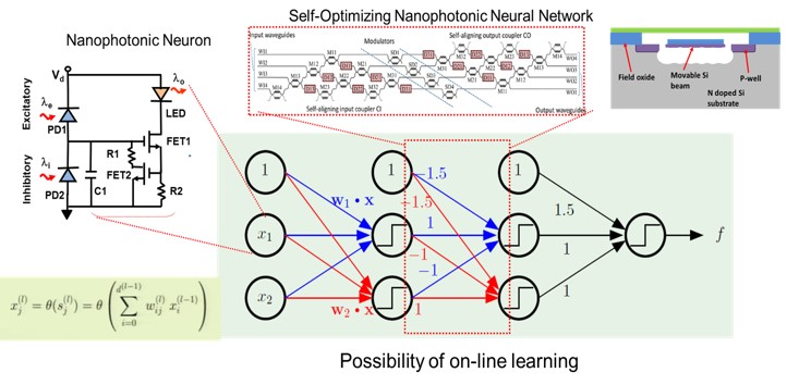
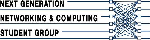
Figure 4 shows an example of the proposed Nanophotonic Neural Network with Nanophotonic Neurons at each node, and the self-optimizing nanophotonic neural network with 2×2 NEMS-MZI between each layer. An important part of a neural computation scheme is some method of providing this necessary set of weighted connections from the neuron outputs and the inputs to the next layer of neurons. The recent “universal linear optical component†that can be built up using a network of 2×2 Mach-Zehnder interferometer blocks connected in a mesh, which we proved to be able to implement any linear transform from its inputs to its outputs.
Importantly, unlike many previous optical schemes, this can be accomplished entirely without having to throw away any of the optical power unless necessary for the desired linear mapping. Furthermore, this network can be set up without calculations and without calibration of the components, based on training it with appropriate sets of input light beams, and based on a sequence of local feedback loops using local mostly-transparent detectors. This ability to train the network can be used to self-configure, self-stabilize, and even self-learn, to realize an on-line and self-learning system.
C. 3D Nano-Integrated-Neuromorphic-Circuit
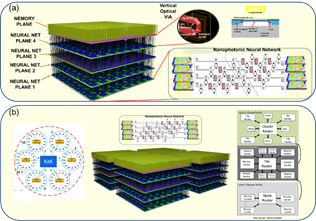
Deep neural networks with many stages or layers can be achieved by 2D and 3D integration of the nano-circuits as illustrated in Figure 5 (a), and can be further scaled out by hierarchical clustering as shown in Figure 5 (b).
MASSIVELY-PARALLEL EMBEDDED PHOTONIC COMPUTING
Von Neumann computing with massively parallel nano-photonic interconnects with nano-electronic logics and NEMS non-volatile memory can also be constructed in a similar manner to complete the system of Figure 1. The complete system can exploit neuromorphic computing to analyze the workload, accelerate floating-point or detailed processing, and to make intelligent decisions based on the learned experiences.
References
[1] R. H. Dennard, et al., IEEE Journal of Solid-State Circuits, vol. 9, no. 5, pp. 256-268, 1974.
[2] P. A. Merolla et al., Science, vol. 345, no. 6197, pp. 668-673, 2014.
[3] D. A. B. Miller, Journal of Lightwave Technology, 2017.
[4] D. A. B. Miller, Optics Letters, vol. 14, no. 2, pp. 146-148, 1989.
[5] D. A. B. Miller, Photonics Research, vol. 1, no. 1, pp. 1-15, 2013.
[6] D. Silver et al.,Nature, vol. 529, no. 7587, pp. 484-489, 2016.
[7] Y. Shen et al., Nat Photon, vol. 11, no. 7, pp. 441-446, 2017.