
Project Overview
The 3D Silicon Photonic LIDAR project seeks to design a large scale, electronically controlled wide angle beam steering device into a single integrated device. In what would be deemed as the most complex electronic-photonic circuit ever fashioned, our team will work to create a wafer-scale system that is 100x smaller and lighter than conventional systems and can steer the optical beam 1,000x faster than mechanical components.
A primary goal of the LIDAR projectis the demonstration of integrated electronic-photonic unit cells that can be tiled together to form large-scale planar apertures. The program calls for devices that are modular and scalable to apertures of up to 10 centimeters in diameter and that can run at 100 watts of optical power. Another primary objective is the operation of a fully-functional, chip-scale LIDAR system capable of three-dimensional (3-D) imaging at a range of 100 meters.
Successful completion of the LIDAR project could enable rapid 3-D scanning using devices smaller than a cell-phone camera, high-speed laser communications without mechanical steering, foliage-penetrating perimeter sensing, remote wind sensing, and long-range 3-D mapping. Such capabilities could, in turn, find applications in intelligence, surveillance, and reconnaissance (ISR), autonomous navigation, optical communication systems, and robotics.
Current Research Activities
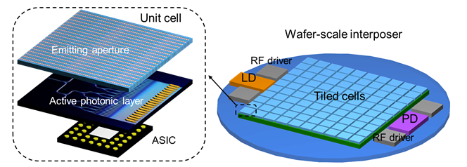
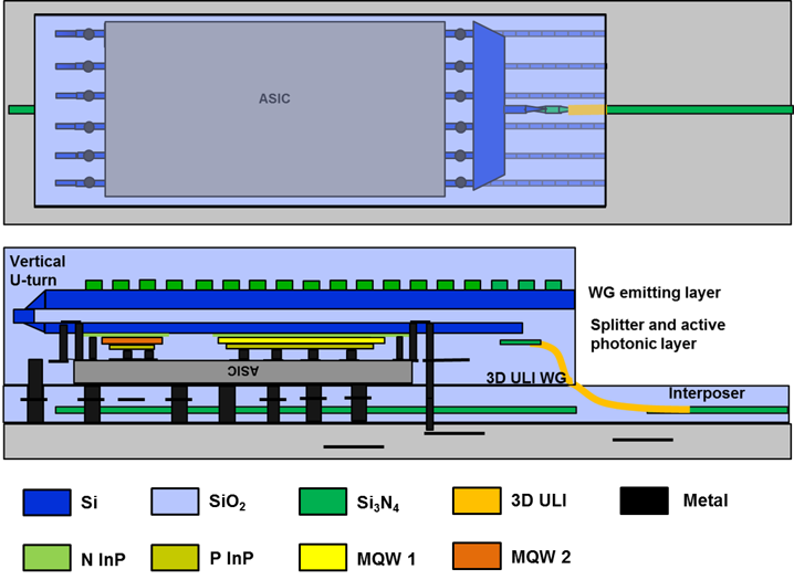
We are particularly focusing our efforts to development of such system in the area of photonic/electronic integrated circuit, namely the cell-based emitters/receivers, integration of the control electronics and wafer-scale interposer. Figure 1 shows the schematic view of the whole PIC/EIC system for the project.
Cell-based emitters/receivers:
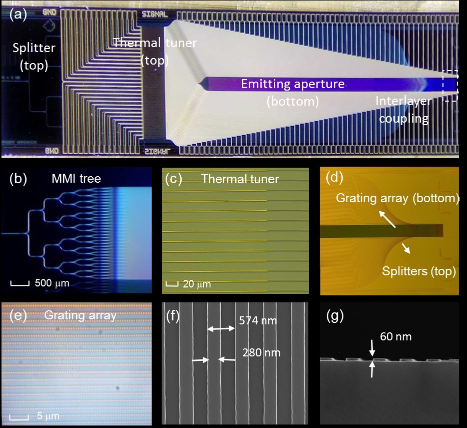
We utilize the waveguides with phase shifters steer in lateral direction (N controls) and tunable laser + fixed grating (1 control point) steers in longitudinal direction to reduce the complexity of the unit cell scaling. The key building blocks of the unit cell includes dense waveguide array, compact and low-loss interlayer optical coupling structures, uniform emitting grating up to 10 mm scale, low power consumption phase modulator and wide range wavelength tunable laser.
Wafer-scale interposer:
We use a wafer-scale interposer to achieve equal power and equal phase power delivery to the 100 tiles of the unit cell with backside electrical connections to the control circuits. Key technologies enables such interposer includes low-loss pathlength matched splitter and waveguide designs, low-loss light coupling from the interposer to each unit cell, integration of the electronic control unit without blocking the aperture, seamlessly integration of the unit cell and thermal control to the interposer.
A.3. Recent Group Publications
[1] Kuanping Shang, Chuan Qin, Yu Zhang, Guangyao Liu, Xian Xiao, Shaoqi Feng, and S. J. B. Yoo, “Uniform emission, constant wavevector silicon grating surface emitter for beam steering with ultra-sharp instantaneous field-of-view”, Optics Express, 2017.
[2] Yu Zhang, Yi-Chun Ling, Kaiqi Zhang, Cale Gentry, David Sadighi, Greg Whaley, James Colosimo, Paul Suni, and S. J. Ben Yoo, “Sub-wavelength-pitch silicon-photonic optical phased array for large field-of-regard coherent optical beam steering“, Optics Express, vol. 27 issue 3 Jan 2019.
[3] Yu Zhang, Yi-Chun Ling, Yichi Zhang, Kuanping Shang, and S. J. Ben Yoo, “High-Density Wafer-Scale 3D silicon-photonic integrated circuits“, JSTQE, 2018