
Technology Overview
The amount of information we process has been continuing its remarkable trend of exponential growth. Sustainably supporting such explosive growth requires scalable, high-yield, and cost-effective integration of microsystems. For two-dimensional electronic integrated circuits (2D EICs), the Moore’s Law stated in mid 1960s [1] that the number of transistors which could be placed inexpensively on an electronic integrated circuit (EIC) doubled approximately every two years. As a corollary, the Dennard’s law [2] claimed that the power-efficiency will also scale at the same pace with the Moore’s law. While this remarkable exponential scalability in integration still continues today after five decades, the Dennard’s law which kept pace with the Moore’s Law for four decades started to fail in 2004. The International Technology Roadmap for Semiconductors (ITRS) [3] mentions a ‘red brick wall’ as there is no known technology solution below the 7 nm technology where complementary metal-oxide-semiconductor (CMOS) scaling is expected to stop (as already noted, CMOS power density scaling stopped in 2004). The two main causes for this limitations are the increases in leakage currents at such small scales (since the atoms don’t scale with CMOS), and the limitations of electronics in interconnects (because of the skin effects and impedances of electronic interconnects). The arrival of chip multi-core processors (CMPs) in 2006 is providing a temporary reprieve in these limitations by offering parallel processing capabilities in multicores without increasing the clock speed. An interesting new trend is the exponential increases in the number of cores in modern processors. In such parallel processing where interconnects are the bottlenecks, photonics provides parallelism and high-capacity independently of distance. Hence, the hybrid integration of photonics and electronics can bring best of both worlds where bosons (photons) and fermions (electrons) exhibit two sets of complementary traits. Photonic integrated circuits (PICs) take advantage of large bandwidth, low latency and low transmission loss, and electrical circuits exploit complicated signal processing. Integration efforts in both EICs and PICs have so far been active primarily in 2D. As the number of transistors exceeded 10 billion per die, high-density integration has extended to 3D integration by stacking multiple layers of 2D EICs using through-silicon-vias (TSVs) [4]. 3D EICs offered a number of performance enhancements over 2D EICs, primarily due to shorter electrical wiring requirements. They in general offer 5 lower power consumption due to reduced number of repeaters and equalizers on shorter communication distances, (b) lower noise and jitter on shorter interconnects, and (c) higher packing density in 3D. In photonics, too, rapid advances in 2D photonic integrated circuits (PICs) have also motivated us to coin a term ‘photonic Moore’s Law [6, 7]’. More recently, 3D photonic integration [8] has emerged as very important steps towards bringing new functionality and higher degrees of integration to microsystems.
At UC Davis, we have recently developed 3D through-silicon-optical-vias (3D photonic TSVs) that can be co-integrated with silicon photonics and CMOS. Utilizing standard CMOS processes enhanced by wafer-bonding available at UC Davis and UC Berkeley cleanrooms, we have designed and demonstrated 3D vertical U-turn devices that will be a platform for the 3D photonic TSVs that can co-exist with standard silicon photonic and silicon electronic integrated circuits with conventional electronic TSVs. This technology will fundamentally change the landscape of computing, networking, and imaging systems by offering high functionality, capacity, and energy-efficiency. This technology can be incorporated into interposers to realize 3D photonic-electronic integrated interposers as well. By prototyping a new generation of interposers and 3D EPICs, we are currently developing new microsystems in computing/networking/imaging enabled by this new technology.
Current Research Activities
– Vertical U-shaped couplers and Silicon Photonic TSVs
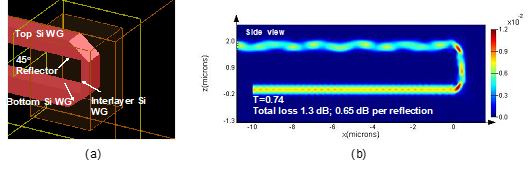
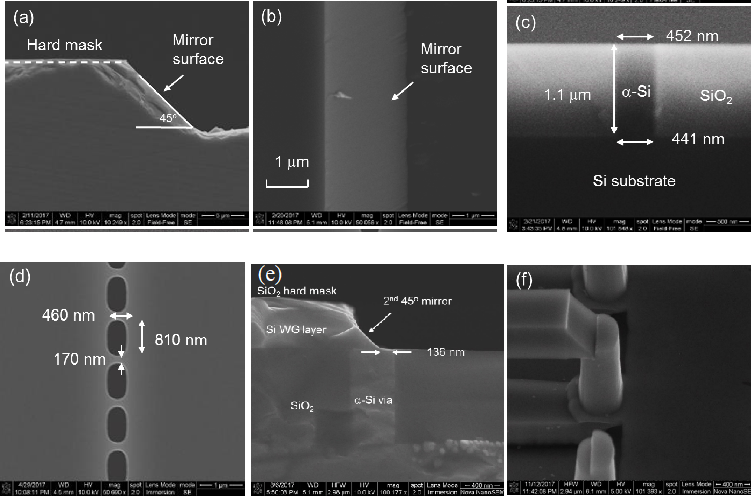
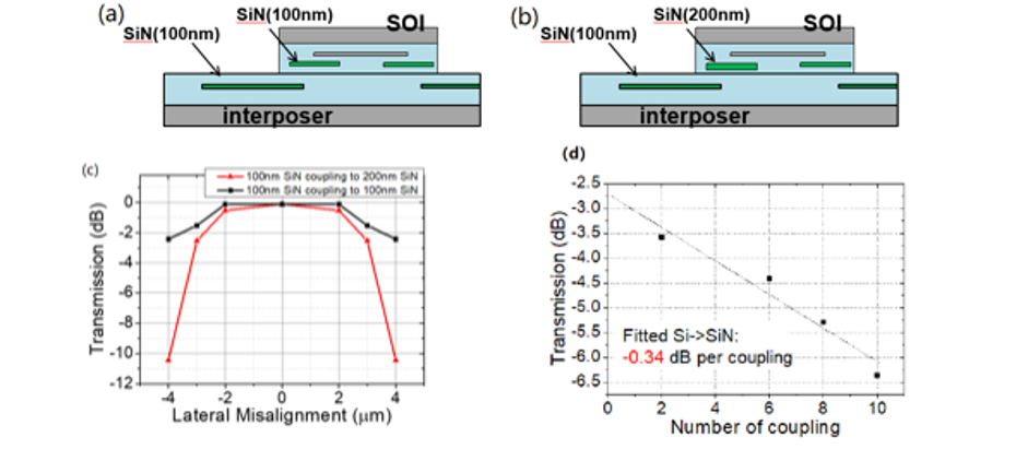
We have designed, fabricated, and demonstrated a silicon photonic U-shaped couplers that can be developed towards silicon photonic TSVs [9, 10]. Figure 1 shows (a) a prospective schematic and (b) FDTD simulated transmission of the vertical U-shaped coupler from the bottom layer to the top layer. We obtained a maximum transmission of 0.74 or 1.3 dB loss from layer to layer, and possible improvement is possible with mode engineering. Figure 2 shows Vertical U-shaped couplers and photonic TSVs fabricated at UC Davis: (a) Cross-sectional and (b) 45o tilted view SEM pictures of an etched 45o reflector. (c) Cross-sectional and (d) top view SEM pictures of fabricated vertical optical vias with 1 ï€ ïm pitch. (e) Cross-sectional and (f) 15o tilted view SEM pictures of fabricated U-shaped coupler structure with 2 um pitch.
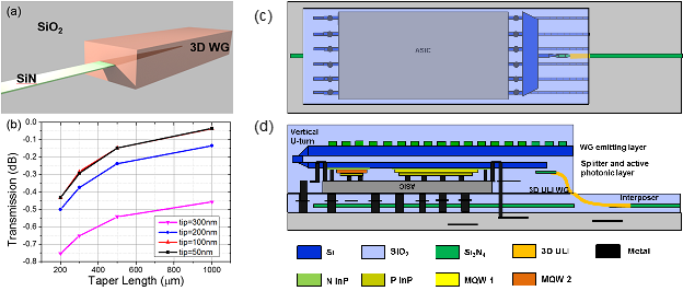
– 3D Electronic-Photonic Integrated Circuits
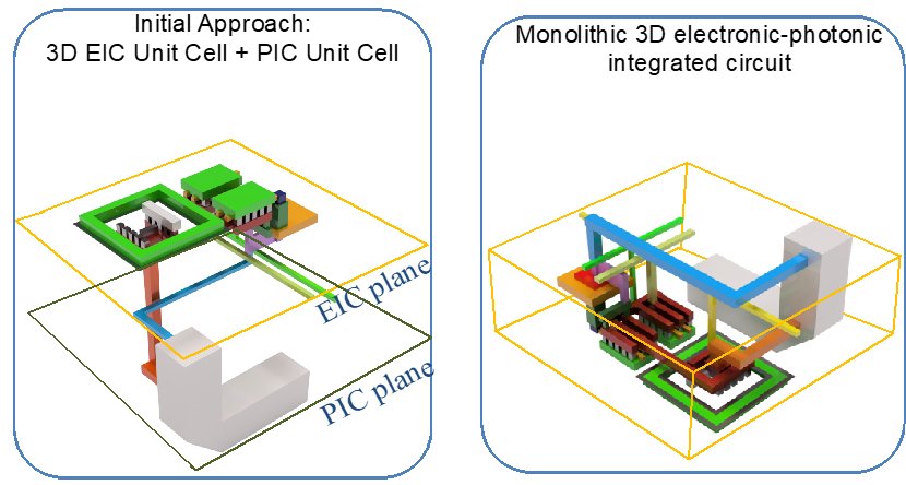
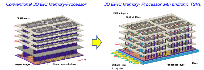
Figure 3 shows schematics of our current efforts taking two parallel approaches for realizing 3D electronic-photonic integrated circuits. The initial approach is to utilize 3D integration techniques such as DBI bonding to achieve cell by cell vertical integration of EICs and PICs, while ultimate approach of monolithic heterogeneously integrated 3D EPIC is being developed. The heterogeneous integration allows III-V lasers, amplifiers, as well as LiNbO3 electro-optical devices together with silicon photonic and CMOS devices. Successful progress will help realize 3D memory-processors, sensing, imaging, and information processing microsystems. Figure 4 shows an example of 3D memory-processor stacks based on conventional methods with electronic ICs vs our proposed 3D EPIC based methods that can bring substantial improvements in energy-efficiency, throughput, and bandwidth [11-13].
– 3D Electronic-Photonic Interposers
Our group has been prototyping various 3D electronic photonic interposers with electrical TSVs, photonic TSVs, and electronic and photonic components for various applications [10, 14-17]. Figure 5 and Figure 6 show some of the examples. 3D ultrafast laser inscription techniques combined with the multilayer 3D photonic-electronic integration methods offer ultimate flexibility in design and functionalities, and additional heterogeneous integration offers ultimate and diverse capabilities by including photonic gain and electro-optical modulation capabilities.
References and Recent Group Publications
- Moore, G.E., Cramming more components onto integrated circuits. Electronics, 1965. Volume 38(Number 8).
- Dennard, R.H., et al., DESIGN OF ION-IMPLANTED MOSFETS WITH VERY SMALL PHYSICAL DIMENSIONS. IEEE Journal of Solid-State Circuits, 1974. SC 9(5): p. 256-268.
- Savchenkov, A.A., et al., Optical resonators with ten million finesse. Optics Express, 2007. 15(11): p. 6768-6773.
- Emma, P.G. and E. Kursun, Is 3D chip technology the next growth engine for performance improvement? IBM Journal of Research and Development, 2008. 52(6): p. 541-552.
- Topol, A.W., et al., Three-dimensional integrated circuits. IBM Journal of Research and Development, 2006. 50(4.5): p. 491-506.
- Thylén, L., et al., The Moore’s Law for photonic integrated circuits. Journal of Zhejiang University SCIENCE A, 2006. 7(12): p. 1961-1967.
- Smit, M., J. van der Tol, and M. Hill, Moore’s law in photonics. Laser & Photonics Reviews, 2012. 6(1): p. 1-13.
- Yoo, S.J.B., B. Guan, and R.P. Scott, Heterogeneous 2D/3D photonic integrated microsystems. Microsystems & Nanoengineering, 2016. 2: p. 16030.
- Zhang, Y., et al. 3D integrated silicon photonic unit cell with vertical U-turn for scalable optical phase array. in Conference on Lasers and Electro-Optics. 2018. San Jose, California: Optical Society of America.
- Zhang, Y., et al., High-Density Wafer-Scale 3-D Silicon-Photonic Integrated Circuits. IEEE Journal of Selected Topics in Quantum Electronics, 2018. 24(6): p. 1-10.
- Yoo, S.B. 3D integrated photonic technologies for future functional microsystems. in CLEO: Science and Innovations. 2016. Optical Society of America.
- Grani, P., et al., Photonic Interconnects for Interposer-based 2.5D/3D Integrated Systems on a Chip, in Proceedings of the Second International Symposium on Memory Systems. 2016, ACM: Alexandria, VA, USA. p. 377-386.
- Shang, K., et al. Ultra-Low Loss Vertical Optical Couplers for 3D Photonic Integrated Circuits. in Optical Fiber Communication Conference. 2015. Los Angeles, California: Optical Society of America.
- Fotouhi, P., et al., Enabling Scalable Disintegrated Computing Systems With AWGR-Based 2.5D Interconnection Networks. IEEE/OSA Journal of Optical Communications and Networking, 2019. 11(7): p. 333-346.
- Zhang, Y., et al., Foundry-Enabled Scalable All-to-All Optical Interconnects Using Silicon Nitride Arrayed Waveguide Router Interposers and Silicon Photonic Transceivers. IEEE Journal of Selected Topics in Quantum Electronics, 2019. 25(5): p. 1-9.
- Xiao, X., et al. Scalable AWGR-based All-to-All Optical Interconnects with 2.5D/3D Integrated Optical Interposers. in 2018 IEEE Photonics Society Summer Topical Meeting Series (SUM). 2018.
- Ling, Y.-C., Y. Zhang, and S.J. Ben Yoo. Arbitrary vertical low-loss waveguides in deposited oxide of optical interposers for low-loss 3D photonic packaging. in Conference on Lasers and Electro-Optics. 2018. San Jose, California: Optical Society of America.