Technology Overview
There are two main methods of realizing 3D PICs. The first method utilizing ultrafast laser inscription (ULI) offers freeform shaping of waveguides in arbitrary contours and formations. The second method utilizing multi-layer stacking and coupling of planar PICs exploit relatively mature 2D PIC fabrication processes applied to each layer sequentially. Both fabrication methods for 3D PICs have advantages and disadvantages such that certain applications may favor one method over the other. On the other hand, a joining of 2D PICs with 3D PICs can help realize integrated microsystems of new functionalities such as non-mechanical beam steering, space-division multiplexing (SDM), programmable arbitrary beam shaping, and photonic signal processing. We discuss examples of 3D PICs and 2D/3D integrated PICs in two applications, SDM via orbital-angular-momentum (OAM) multiplexing/demultiplexing and optical beam steering using optical phased arrays.
Perhaps the most distinctive 3D PICs with no electronic counterpart is realized by 3D waveguide formation by ultrafast laser inscription (ULI). Direct laser writing of waveguides in dielectric material is an extremely powerful fabrication technique [34]. It utilizes the multi-photon nonlinear absorption of sub-bandgap photons to create permanent structural changes in a material with dimensions comparable to the writing laser’s wavelength (e.g., ~1 µm3). The types of structural changes include refractive index and an increased susceptibility to chemical etching [35]. The induced modifications from a femto-second train of optical pulses are strongly localized in three dimensions to the high intensity region at the focus of a lens driven by a nonlinear absorption mechanism. This unique characteristic is what provides direct laser writing its unique advantage over other waveguide fabrication techniques; the capability to freely form truly three-dimensional structures [36]. ULI has been widely demonstrated in many types of materials including amorphous glasses and crystals with measured propagation losses ≤0.3 dB/cm [37, 38] in fused silica.
Current Research Activities
3D multi-ring waveguides for OAM applications
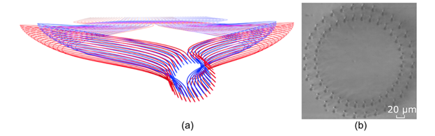
Multi-ring 3D waveguide design and fabrication for the OAM application are important first step towards scalable spatial division multiplexing (SDM). Our group has developed a 3D waveguide design tool utilizing the routing algorithm that maintains the same photonic path lengths, the minimum radius of curvature, and the minimum inter-waveguide distance. Figure 6 (a) shows the computer-aided-design, and (b) a photograph of the fabricated multi-ring 3D waveguides at the facet. In such cases, the multi-ring OAM PICs can possibly realize generation of arbitrary spatial waveforms such as Laguerre-Gaussian modes by adding the radial control of the optical field to the azimuthal control achieved in individual OAM PICs of each ring.
3D waveguides for optical phased arrays and beam steering
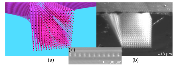
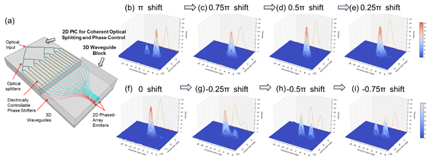
In addition to the spatial waveform shaping using multi-ring 3-D PICs fabricated by ULI methods, the same ULI can form 3-D PICs of arbitrary array shapes, including a rectangular array. Figure 7 shows the details of a 3-D PIC that transforms a linear 1 × 256 input waveguide array to a 16 × 16 rectangular array of output waveguides using the ULI technique. Figure 7 (a) show a computer aided design with detail of the output array, (b) a photograph of the output facet and (c) photograph of a portion of the input facet. As is the case with most dielectric waveguides, the index difference between the waveguide core and cladding determines the minimum bending radius due to radiation losses from the bent waveguide. Since the index difference for these ULI waveguides is ~0.5%, we chose a minimum bending radius of 20 mm, which showed negligible bending loss. Similarly to the multi-ring 3-D PICs, the rectangular PICs also utilized the 3D computer aided design for precise optical path length matching of all 256 waveguides. Such 3D PICs are useful for non-mechanical beam steering [51] as well as SDM MIMO optical communications and beam forming (e.g. Hermite-Gaussian modes). Figure 8 (a) shows an example of optical beam steering realized by hetergneous integration of such a 3D waveguide array and a 2D PIC consisting of optical splitter waveguides and waveguide array phase shifters. Figure 8 (b-i) illustrates optical beam steering results experimentally obrained from phase tuning the array waveguides in the 2D PIC by π, 0.75π, 0.5π, 0.25π, 0, -0.25π, -0.5π, and -0.75π between the waveguides [51]. Here, phase error correction [11] is conducted by phase tuning the array waveguides.
3D Photonic Packaging
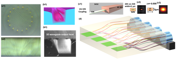
The most scalable solutions to high-density MCF interface for silicon photonics is to utilize 3D ultrafast laser inscription capabilities. UCDavis has developed low-loss (0.1~0.2 dB/cm) ULI capabilities for arbitrarily shaped 3D waveguides capable of low loss (< 0.3 dB) MCF coupling using 3D CAD design tools with compatible design-rule checks. Figure 5 (a) and (b) show 16 core 3D ULI waveguides and 256 3D ULI waveguides designed to interface specialty MCFs to silicon photonic waveguides on the other end. In particular, UCDavis demonstrated ULI directly on an oxide dielectric layer deposited on silicon wafers. Hence, as Figure 5 (d) illustrates we propose to develop a silicon photonic 3D fan-out chip interfacing an array of MCFs with an array of silicon nitride waveguides with the 3D ULI waveguides (shown example shows 4 strands of 8-core MCFs interfacing with a silicon photonic transceiver die which will also have a matching 32 silicon nitride waveguide interface.
UC Davis has recently demonstrated an optical interposer with vertical evanescent waveguide coupling to a silicon photonic die with 0.38 dB loss (limited by the airgap caused by the non-planar metal layer) providing ± 2 µm alignment tolerance. Elimination of the airgap at the planarized interface expects to reduce the optical loss to below 0.1 dB. Wafer-scale fabrication of 3D ULI is possible utilizing UC Davis’ fabrication method, especially because the optical beam can be split to multiple spots (100 spots is possible at the current laser power level and the required power for the ULI) for simultaneous writing of multiple spots. From the CAD design to actual completion takes only several hours, and the proposed method is viable for rapid prototyping. Foundry transition to AIM Photonics have been discussed multiple times over the past two years with keen interest from the AIM Photonics community including industry members.
References