
Technology Overview
Silicon photonics is a transformative enabling technology that brings parallelism, high throughput, power efficiency, and cost-effectiveness to computing. Integration and packaging between silicon photonics and silicon CMOS components can exploit 2D, 2.5D, or 3D as well as even monolithic integration technologies thanks to the compatibility between the two utilizing the form factors of silicon electronics.
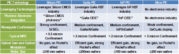
Recently, both electronic integrated circuits (EICs) and photonic integrated circuits (PICs) have been seeking heterogeneous integration. Modern EICs often integrate heterogeneous circuits involving analog and digital, or involving silicon CMOS and Ge bipolar transistor circuits. Likewise, photonic integration also benefits from integrating heterogeneous materials While silicon photonics is rapidly emerging as a viable and possibly ubiquitous photonic integration platform, silicon lacks optical gain, Pockel’s effect, and Faraday effect useful for realizing lasers, phase modulators, and non-reciprocal devices. Hence, the co-integration of silicon with III-V materials, electro-optical dielectrics, and magneto-optical materials can greatly enhance the functionalities of heterogeneously integrated microsystems. Table 1 illustrates various photonic integration platforms indicating benefits from heterogeneous integration.
Heterogeneous integration can be achieved by either monolithic integration or hybrid integration. In particular, monolithic integration by hetero-epitaxy is attractive in that it can exploit large host substrates (e.g. silicon wafers) and epitaxially grow III-V or other compound materials on a wafer-scale at dimensions defined by the host substrate. Overall, monolithic integration by heteroepitaxy remains challenging for achieving low-defect heterogeneous integration. In contrast to monolithic integration, hybrid integration methods do not attempt material growth but utilize various bonding mechanisms between dissimilar (or similar) materials already grown on individual substrates. At UC Davis, we pursue heterogeneous integration by various methods including wafer bonding, micro-transfer printing, and special deposition techniques to integrate III-V, LiNbO3, and other specialty materials.
Current Research Activities
Hybrid III-V/Si Lasers and Optical Amplifiers
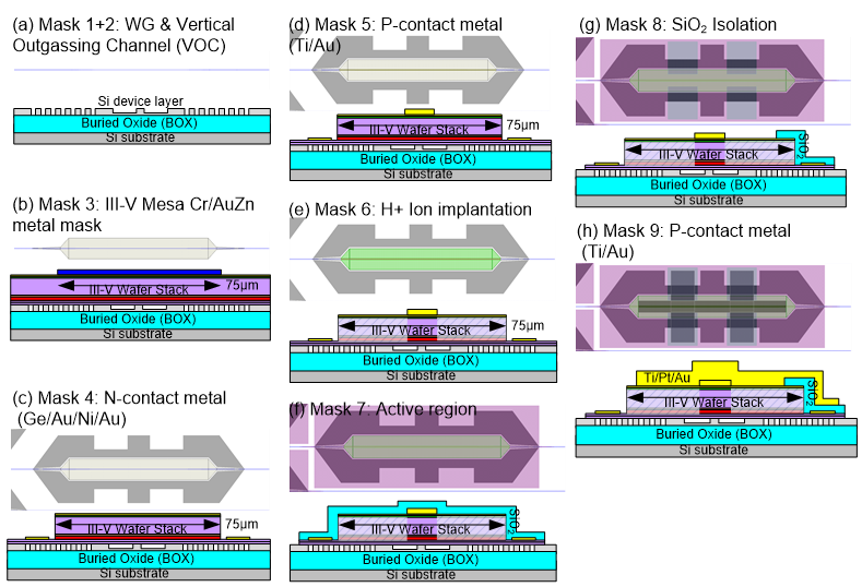
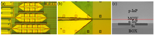
Utilizing wafer-bonding methods, we designed, fabricated, and demonstrated the record efficiency of semiconductor optical amplifiers at 1550 nm on silicon. As shown in Figure 1, fabrication at UC Davis and UC Berkeley cleanrooms begins with a 150 mm diameter silicon-on-insulator (SOI) wafer which consists of a 500 nm thick top silicon layer and a 3 μmA buried oxide (BOX). The wafer goes through initial RCA-1 and RCA-2 cleaning and is then coated with 400 nm of Rohm Haas UV210-0.6 photoresist, soft-based at 130º C for 60 seconds, and then exposed with an ASML PAS 5500 300 deep-UV lithography stepper using a 248nm-KrF light source at 18mJ/cm2 with appropriate focus correction. The details of the fabrication steps are described in reference [1, 2]. Figure 2 shows the completed hybrid InP/Si SOAs.
Hybrid LiNbO3 waveguides on silicon substrate
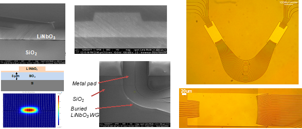
Lithium Niobate crystals offer a number of attractive properties for optical devices, including wide transparency windows, large electro-optic effects, and high second-order susceptibilities [3]. Conventional LiNbO3 devices have been widely used for high-performance light modulators [4, 5]. However, these devices are fabricated by diffusion or ion-exchange waveguide fabrication processes, leading to relatively large footprints and large VÏ€ due to the small refractive index contrast between the core and cladding. Recently, the heterogeneous integration of LiNbO3 thin-film on insulators [6, 7] has attracted strong interest as a new platform for compact photonic integrated circuits (PICs). It allows for reducing the size of the devices thanks to stronger light confinement using higher refractive index contrast. Motivated by these advantages, we design complementary building blocks oriented for light filtering compatible with large-scale integration. We can envisage to enable wavelength-division-multiplexing on-chip for this platform.
As illustrated in Figure 3[8] we designed, fabricated, and demonstrated low-loss Array Waveguide Gratings (AWG) on a compact LiNbO3 platform. Based on this platform, we designed an 8—500 GHz LiNbO3 AWG. The device is composed of two star-couplers and an array of waveguides with a linear increment of the optical path lengths. The typical footprint of the device is 5— 3 mm2.
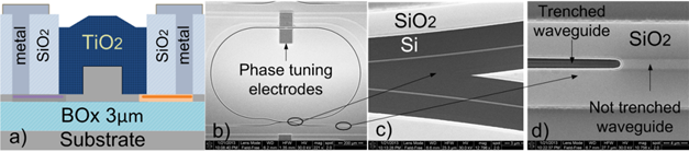
CMOS-Compatible Athermal Silicon Photonics
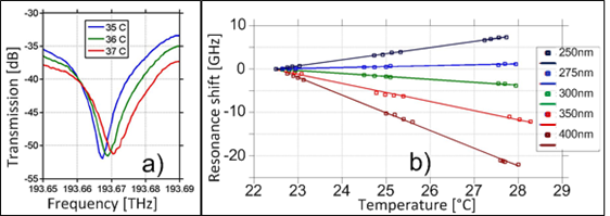
Silicon photonic devices are sensitive to environmental temperature variations since silicon has a relatively large thermo-optical coefficient (TOC) of ~1.84—10°C. One method of thermal stabilization is to adopt an upper cladding made of a material with negative TOC to compensate for the positive TOC of silicon. Titanium dioxide has a strong negative TOC of ~-(1~2)—10°C and is compatible with CMOS processes offering superior reliability than polymers, thus it has been attracting strong interest. We designed, fabricated, and tested athermal silicon waveguides clad with TiO2 Â with athermal characteristics at 1550 nm and also additional devices with temperature-dependent resonant wavelength shifts less than 5 pm/°C exhibiting second-order effects near 1310 nm{Feng, 2014 #3082;Shang, 2013 #2986;Djordjevic, 2013 #2994;Djordjevic, 2012 #2985; Zhou, 2009 #2317;Zhou, 2009 #2322}.
References