
Project Overview
The mid-infrared (MWIR) and long-wave-infrared (LWIR) optical phase arrays (OPAs) are attractive for gas-sensing or thermal LIDARs and for FSOC with lower sensitivity to turbulence and scintillation. While exploiting the transparent transmission window of the atmosphere and high eye-safety optical power at the operating mid-IR wavelengths, the range of the OPA devices can be further increased. The emergence of quantum cascade laser (QCL) made easier to address MWIR and LWIR spectral range. QCL sources are achieving high-efficiency and high continuous wave-power. However, the mature silicon photonic platform used for advanced and complex PICs is incompatible with MWIR. In this project, we pursue MWIR and LWIR OPAs based on Germanium-Silicon based 3D Photonic and Electronic Integrated Circuits (EPICs).
The fabrication process involving Ge on silicon can utilize the CMOS fabrication platform to achieve tolerance and resolution sufficiently large creating subwavelength (λ/2) MWIR structures needed for high-performance LIDARs
Current Research Activities
As in the SiPhotonic LIDARs, we are particularly interested in development of such systems in the area of 3D EPIC development where each cell includes emitters/receivers, and the control electronics.
Cell-based emitters/receivers:
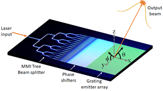
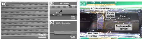
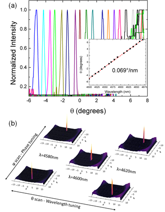
As in the SiPhotonic LIDARs, we utilize the waveguides with phase shifters steer in lateral direction (N controls) and tunable laser + fixed grating (1 control point) steers in longitudinal direction to reduce the complexity of the unit cell scaling. The key building blocks of the unit cell includes dense waveguide array, compact and low-loss interlayer optical coupling structures, uniform emitting grating up to 10 mm scale, low power consumption phase modulators and wide range wavelength tunable lasers. Figure 1 shows a schematic view of the MWIR/LWIR Ge-Si OPA Photonic Integrated Circuit, and Figure 2 shows photographs of fabricated chips, and Figure 3 shows normalized far-field patterns of the beam steering experimental results.
A.3. Recent Group Publications
- Mathias Prost, Yi-Chun Ling, Semih Cakmakyapan, Yu Zhang, Kaiqi Zhang, Junjie Hu, Yichi Zhang, and S. J. Ben Yoo, “MWIR Solid-State Optical Phased Array Beam Steering using Germanium-Silicon Photonic Platform,†IEEE Photonics Journal, 2019
- Mathias Prost, Yi-Chun Ling, Semih Cakmakyapan, Yu Zhang, Kaiqi Zhang, Junjie Hu, Yichi Zhang, and S. J. Ben Yoo, “MWIR Solid-State Optical Phased Array Beam Steering using Germanium-Silicon Photonic Platform“, OFC , Mar 2019
I am wondering about typical static power consumption of such imaging photonic chip. Have you adapted any special approach to reduce DC power consumptions as many thermal phase shifters are used in this architecture. I would like to know any thoughts on this topic.
Hi Ranjan,
Thank you for your interest in the imaging project. Sorry for the late reply. Could you please ask your question directly to one of the NGNCS group members working on the project, check the related paper for email?
thanks,
Admin